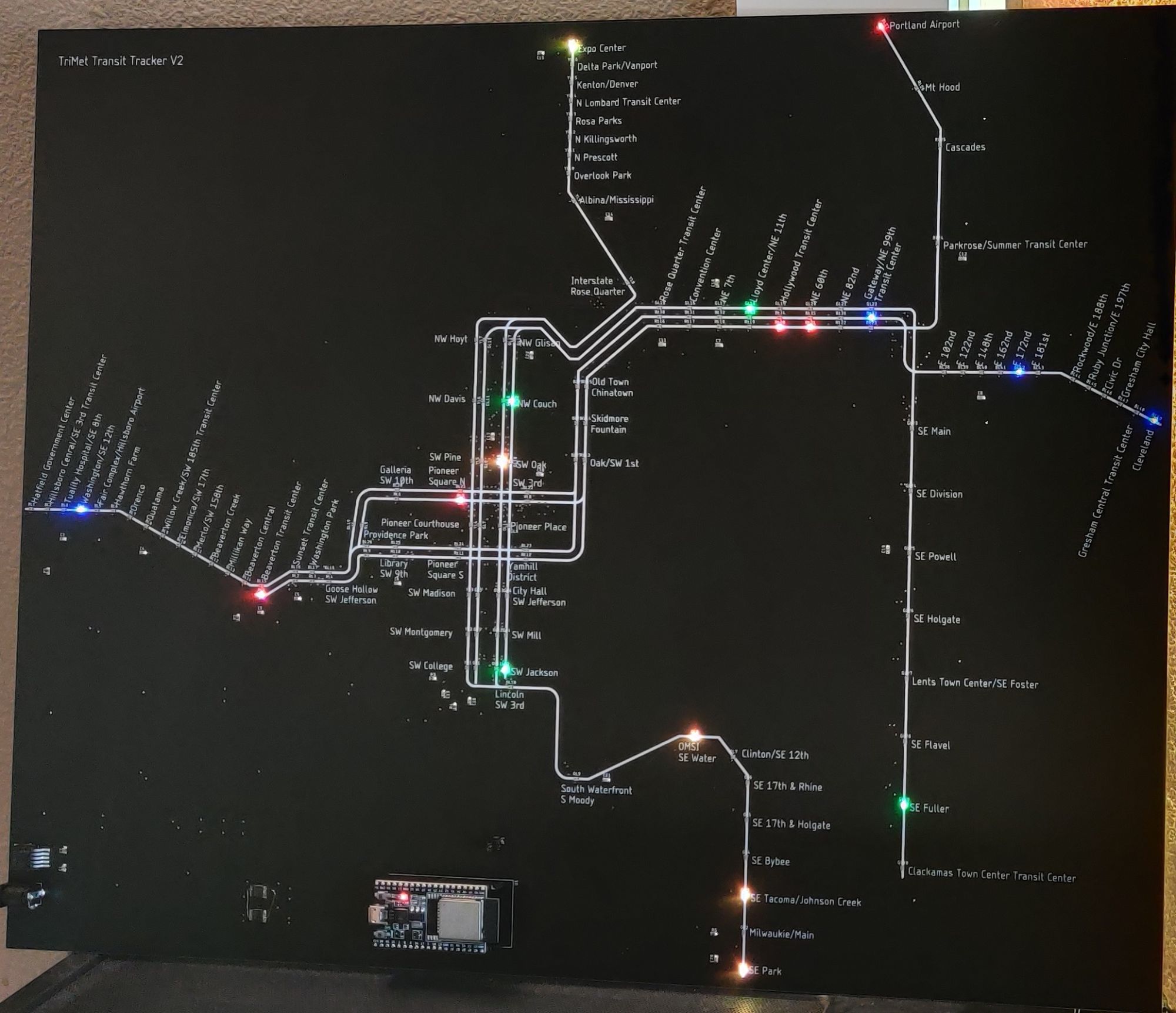
What it is
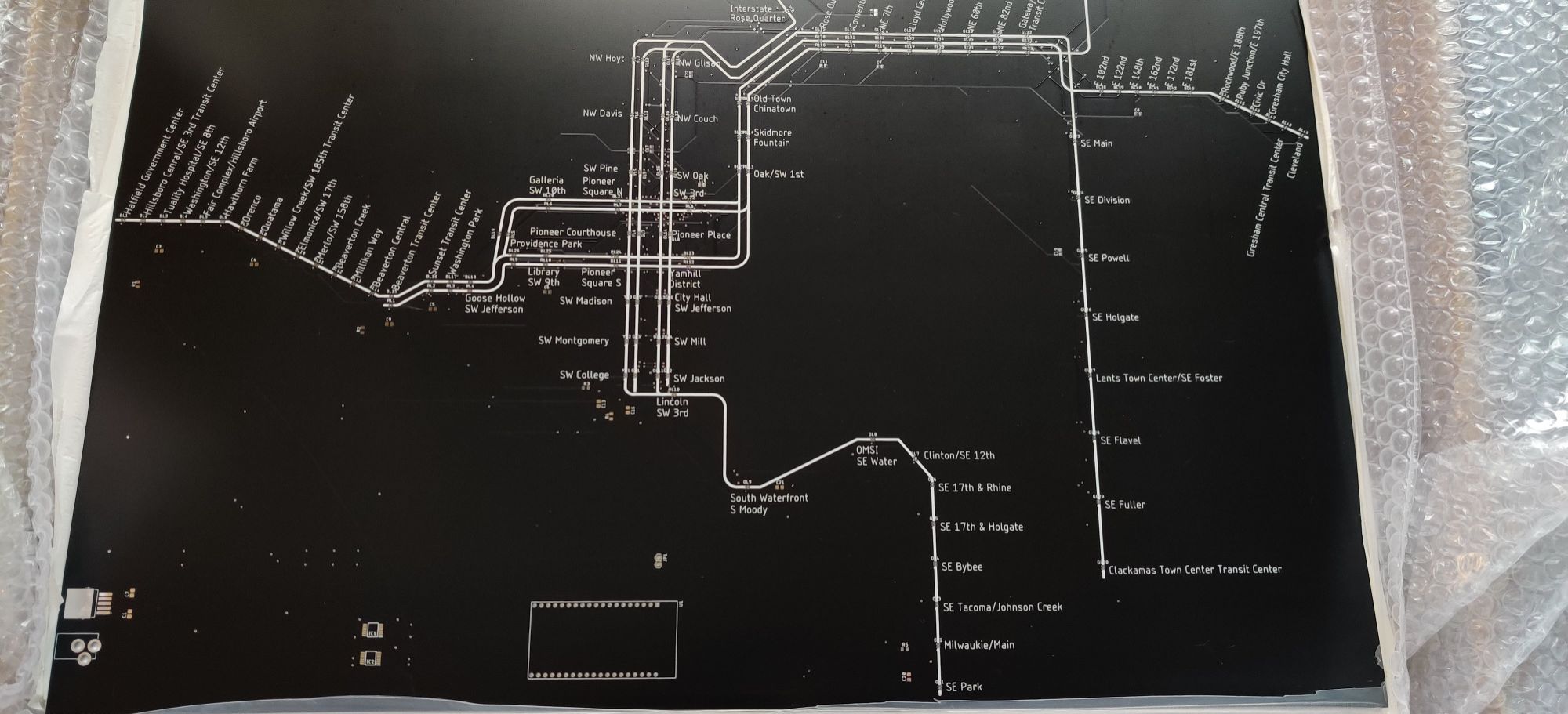
The Portland Transit Tracker is a custom 20"x15" PCB (Printed Circuit Board) that uses the TriMet API to show in real time what MAX stops have a train at them. The layout of the lines on the board match that of the official TriMet transit map. Each station is represented by a colored LED that is the same color as the line is it a part of.
A bill of materials for the board can be found here, and the code, along with instructions on how to flash the board, can be found here.
Inspiration
Inspiration for this project came to me while I was working on the manufacturing floor of one of my previous employers. One of the machines there had a control panel with straight white lines and blue LEDs. At a distance, the panel resembled a train switch board. It was then that I thought it would be cool to build a switchboard like board for the TriMet MAX line, the public transit system in my city.
Designing V1
Initial plans for the project had the path of different rail lines laid out on a PCB with silkscreen lines, and LEDs that traced those different lines. The LEDs would then light up as trains moved through the map. Given the limited number of outputs of small microcontrollers and the high current all the LEDs would draw, I planned to drive the LEDs in sections, but cycle them fast enough as to make it look like they were being powered on all at once.
Once I started designing the project, I realized that given the information that the TriMet API gave and the sheer number of LEDs required to trace the different lines; I decided to move instead to having an LED for each stop along the line. To run the board, I decided on the ESP32 for its WIFI capabilities and relatively small size.
Given that there were a total of 5 different lines (blue, red, yellow, green and orange), and a total of 144 stops, I needed a way to drive the LEDs. I wasn't able to drive all the LEDs directly from the ESP32, given the limited I/O pins, so I decided on using a DEMUX to let one pin control multiple LEDs. Given the nature of a DEMUX, the pin could only power one LED at a time, but that was fine for my use case as I wanted to power the LEDs in sections anyways.
With the LEDs now in groups of 8, I needed some way to keep track of what LED/station was in which group. I then grouped the stations based on adjacency on the official TriMet map. In the end, I was left with the following groupings. I then labeled each LED with following naming convention {color|stationPostionInGroup|group#}. This labeling would come in handy when laying out the board and when coding.
So now as it stands, the max number of LEDs that will be on at the same time will be 18. I decided to go with 0805 LEDs with a current draw of 25mA, so the total current draw is still within reasonable limits when 18 LEDs are being powered on at the same time.
Now I needed a way to trigger the different groupings. I first needed a way to cycle through the DEMUX channels and keep everything in time. What I ended up with was a binary ripple counter set to count up to 0b111 (7) and a clock pulse generated by a 555 timer. The output of the counter would hook up to the channel select pins on the DEMUXes and the clock pulse would go to the counter and the ESP32. It would all work like the following:
- Clock pulses
- Counter increases by one
- This then causes the DEMUXes to switch to the next channel
- This then causes the DEMUXes to switch to the next channel
- An interrupt on the ESP32 would be triggered by the pulse, and would disable the clock
- While the clock is disabled, the ESP32 would write to all 18 pins with a HIGH or LOW depending on whether or not the currently selected station needed to be lit
- Clock is re-enabled
- While the clock is disabled, the ESP32 would write to all 18 pins with a HIGH or LOW depending on whether or not the currently selected station needed to be lit
- Cycle continues
With the general plan finalized, I then went to construct the board in Eagle.
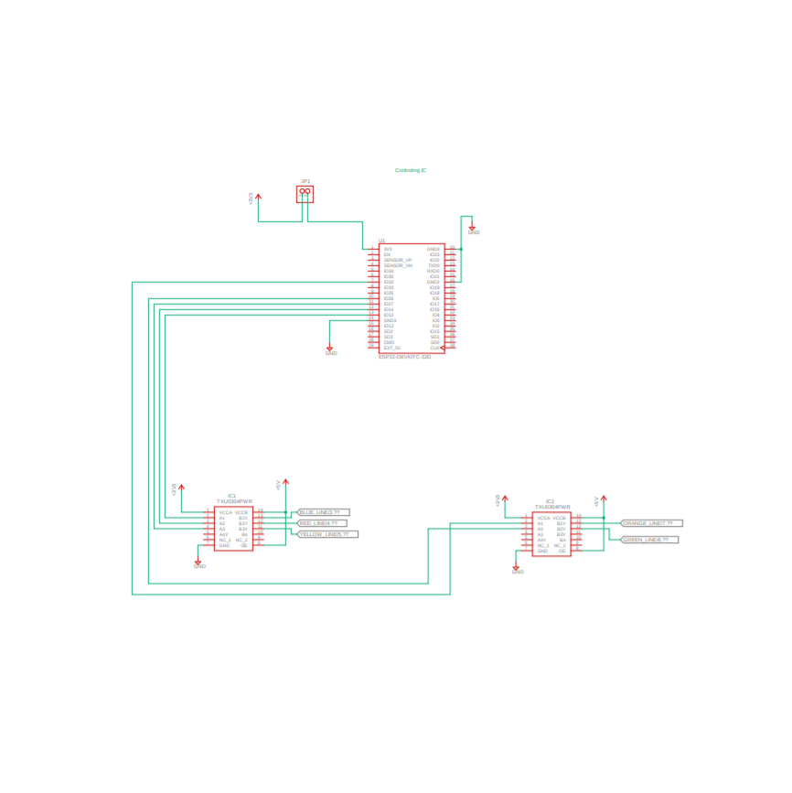
Below is the finalized schematic.

You'll notice that some component values for the 555 timer are left with no values. This is because I planned to fine tune the right frequency with an external frequency generator. Due to this, I also included a jumper pin that would enable me to completely disconnect the 555 timer circuit from the rest of the board and instead hook up my frequency generator.
With that complete I then created the board itself. Below you can see the board before all the traces were routed, and after they were routed (minus the ground planes)
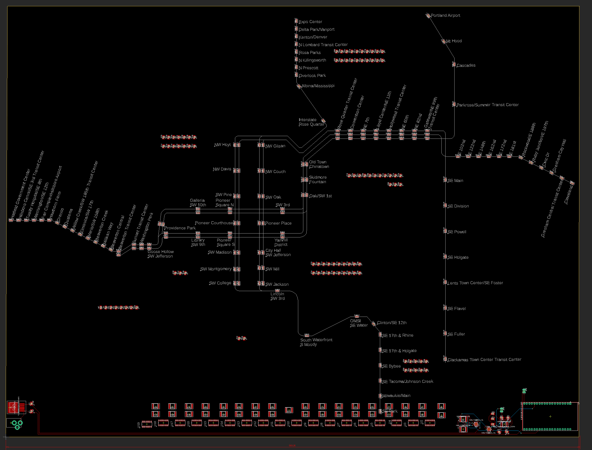

However, before I could manufacture this version, I ended up creating version 2.
Designing V2
While I was finishing up V1 in Eagle, I was already starting to worry about production costs. The board had a size of 567x427mm, and quotes for manufacturing a board that size was in the $300+ range. While I could shrink the board size, I couldn't shrink it too much before ruining the look of the transit map and losing space for the controlling ICs.
Talking to a friend about my project, they reminded me that addressable LEDs existed and that could significantly reduce the part count and in turn the board size. Intrigued, I then went and did some more research on what I’d need. I eventually landed on Adafruit’s NeoPixel Addressable LEDs. They were tiny enough so that they could still fit in the footprint of the 0805 LEDs used in V1, so I didn't have to change the spacing of the map layout. Initially however, I was concerned that going with addressable LEDs would increase code complexity, something I wanted to avoid in this project, but was eventually able to find a library that was compatible with the ESP32. One thing to note however, is that the ESP32 uses 3.3V logic, while the LEDs use 5V logic. To get around this, I ended up choosing to use a voltage translator, specifically the TXU0304PWR.
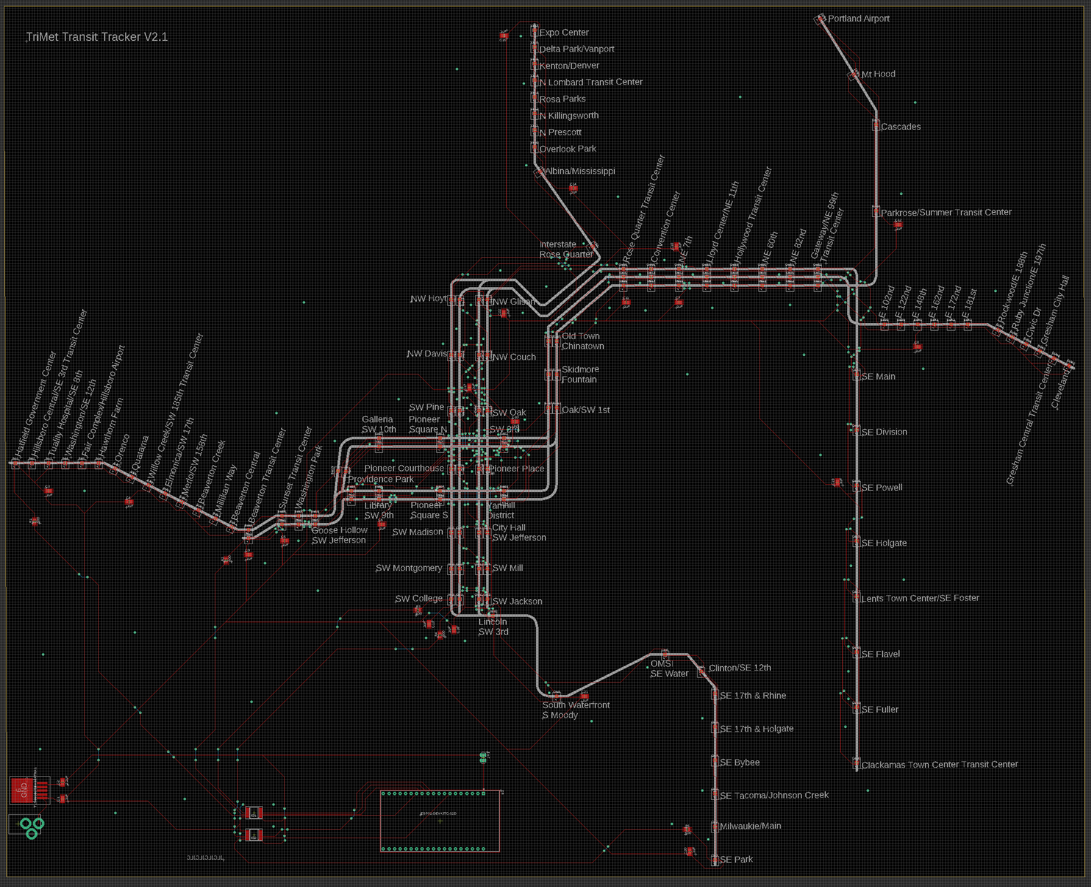
After going back to the schematic, I was able to save the map layout and shrink the board in the Y direction. I could also shrink it a bit more in the X direction, so I reduced some spacing in the map layout, without sacrificing much in terms of overall look.
Below is the finished schematic for V2, as well as the board with traces routed (minus the ground planes).
With the reduction of components, and the ability to shrink the board in the both the X and Y directions, I was able to get the board size down to 494x398mm reducing the production cost to ~$172
To manufacture the board, I ended up going with JLC PCB, as I had used them in the past and was pleased with their quality.
Once the boards arrived, it was time to assemble everything. I opted to go without a solder stencil to save cost, although I ended up regretting that later. Instead of a stencil, my plan was to apply solder paste individually in a 1ml syringe with a 22 gauge nozzle. Due to the size of the board, I also wasn't able to use a reflow oven. I could have used a cooking oven, but didn't want to gamble with the chemicals that would be released from the flux and binding agents. Instead I opted for a hot air reflow gun.
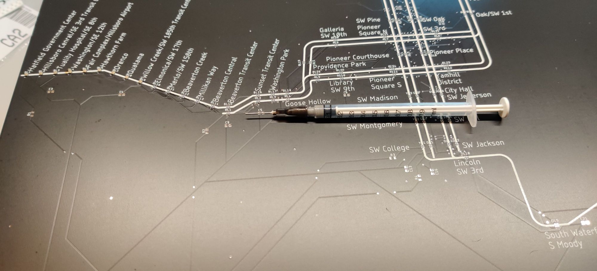
Assembling everything was a tedious and time consuming task. I started with the LEDs first, doing about 6 at a time. In order for the solder paste to stick well to the pads, I had to preheat them with the heart gun before placing down the paste. After that, I would place each LED, then hit them with the heart.
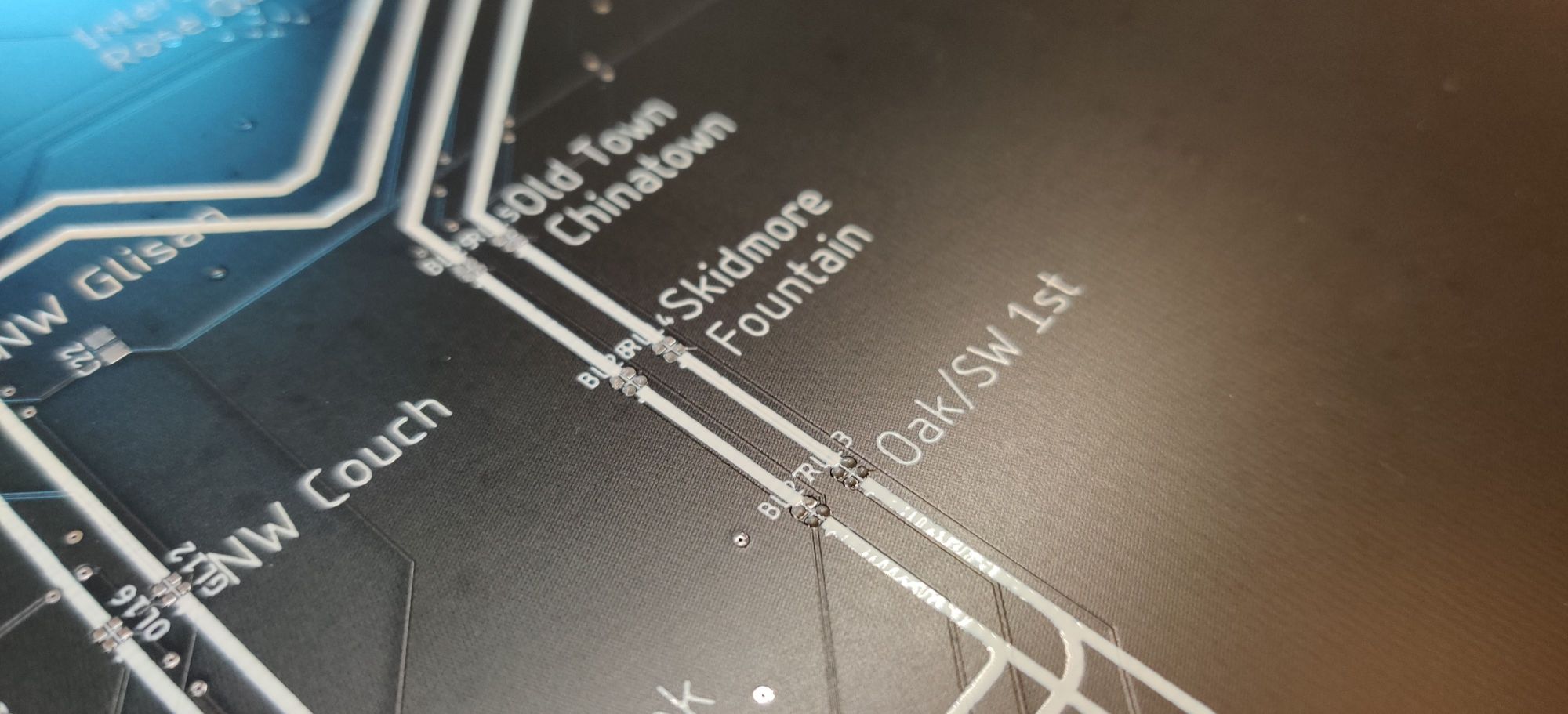
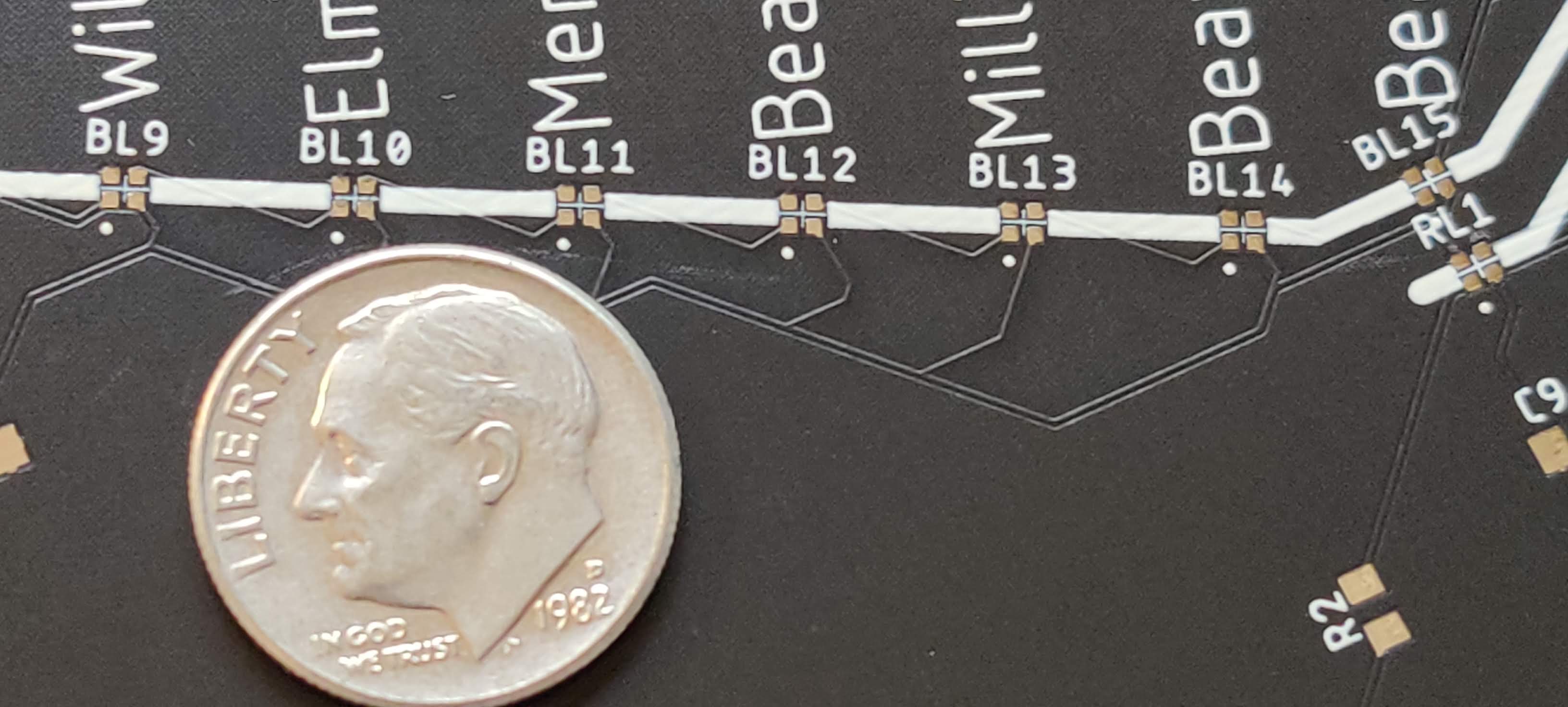
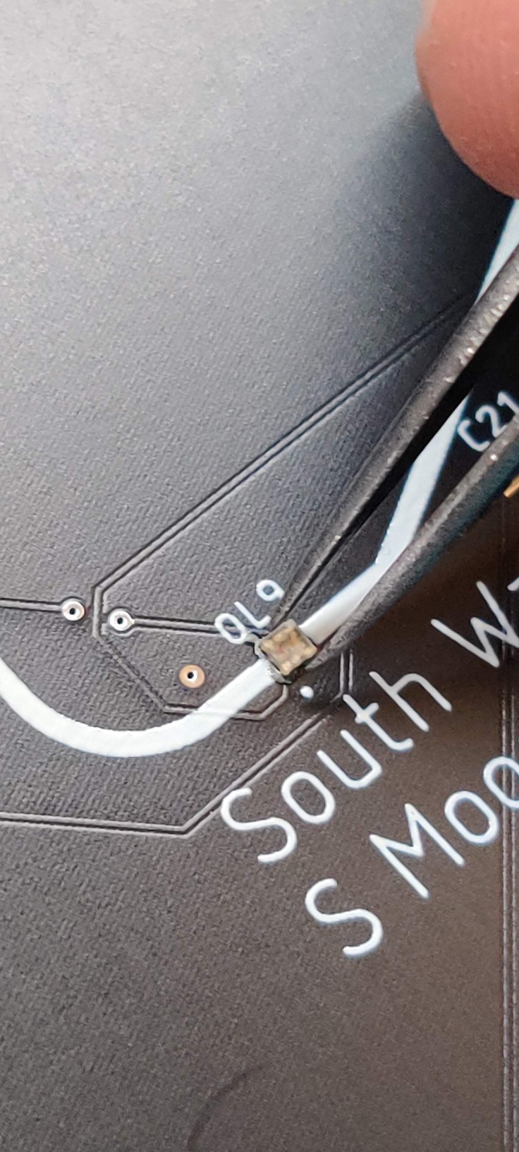
Due to the pads of the LEDs being mounted underneath the package, I had no way of testing connections after they were soldered. The only connection I could test, were shorts between ground and power. Luckily I didn't have any shorts. Overall it took about 10 hours to get everything soldered, and I regretted not getting a stencil.
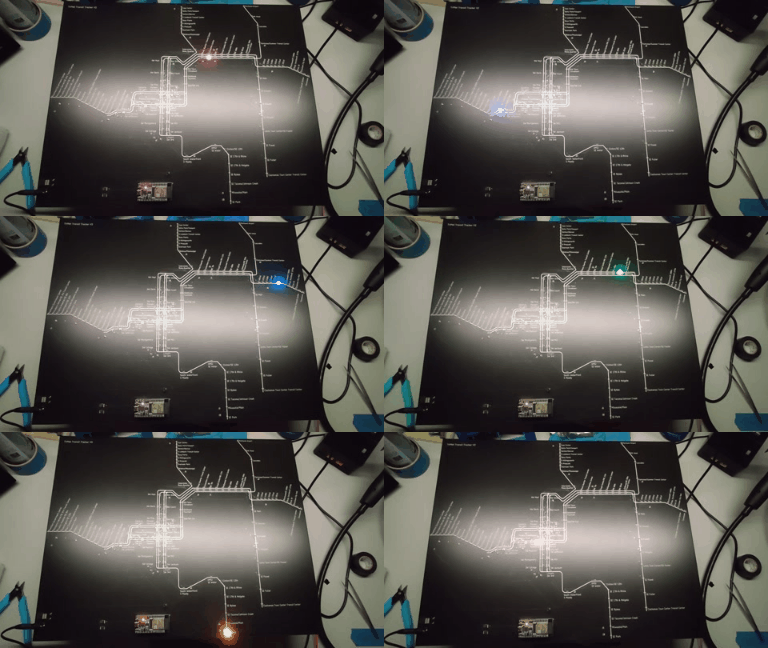
Once everything was soldered, it was time to test. I wrote up a quick program that cycled through all the LEDs, and to my surprise, I only had two LEDs that needed to be reseated which was way less than I was expecting. However, I did discover that I had wired up one of the connections to the first voltage translator incorrectly. Turned out I had misread the datasheet when laying out the board. The voltage translator has four inputs and four outputs. 3 of them go from 3.3V to 5V and the fourth goes from 5V to 3.3V. I however, misread and thought all four went from 3.3V to 5V. Luckily this misread didn't cause any damage, and I had a spare input on the second voltage translator. To fix the issue, I just needed to do some PCB surgery to reroute some connections. I had some copper thread laying around, so I cut the bad trace and soldered jumpers to the proper places. Good as new

Code
I won't go into the code here, as this detailed look has gotten quite lengthy, but you can look at the code here. I have made comments to explain things better.
